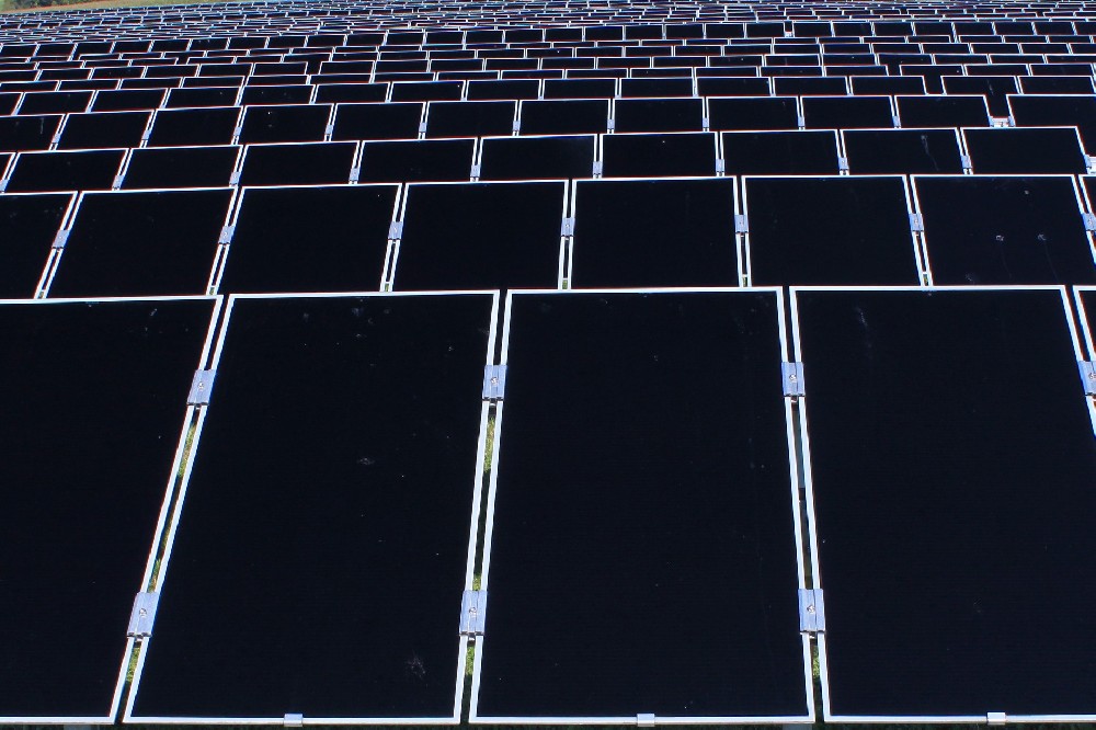

晶体硅电池是由被称为硅片的薄硅片制成的,这些硅片要么是单晶硅( c-Si ),要么是多晶硅( mc-Si ),通常也称为多晶硅( pc-Si )。最近,准单晶片也扩大了可用于太阳能电池制造的衬底材料的选择。为了使太阳能电池正常工作和提高效率,制造过程包括几个专门的生产步骤,其中Lay Tec计量可以做出相当大的贡献。
改进的陷光是通过湿化学电池表面纹理化过程实现的。此外,薄薄的氮化硅( Si N )层形成减反射涂层,使电池具有典型的蓝色至深蓝色甚至黑色外观。为了增加其导电性,对晶体结构进行掺杂。其中p型导电层采用硼掺杂设计,n型导电层采用磷掺杂设计。在电池正面,电接触磨粒条将电荷载流子从薄导体的晶格结构中传导出去,并在称为母线的宽金属条中相遇。在背面,一个大的铝涂层形成了电池后部的接触。

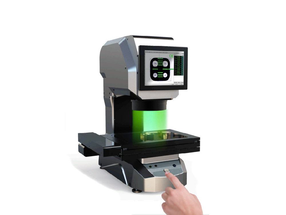
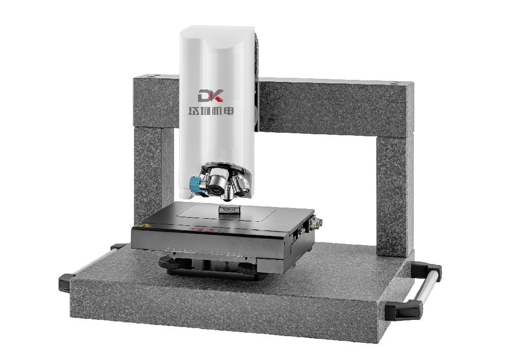
Lay Tec公司的在线计量系统为单晶c - Si太阳能电池生产过程中的各种参数提供了精密和高精度的监测:
● 晶片厚度测量
● 刻蚀步骤后的 织构分析
● 层厚度和钝化层折射率
● 铝背接触层电导率测量
英文:
Crystalline silicon cells are manufactured from razor-thin slices of silicon, called wafers, that are either mono-crystalline (c-Si) or multi-crystalline (mc-Si), often known also as poly-crystalline (pc-Si). Recently, quasi mono-crystalline wafers have also expanded the choice of substrate materials available for solar cell manufacturing. To enable proper function and increase efficiency of solar cells, the manufacturing process comprises several specialized production steps in which LayTec metrology can make considerable contributions.
Improved light trapping is achieved with a wet chemical cell surface texturization process. Additionally, a thinly deposited silicon nitride (SiN) layer forms the anti-reflective coating which gives the cell its typically blue to dark blue or even black appearance. In order to increase its conductivity, the crystal structure is doped. The p-type conductive layer is designed by doping with boron, the n-type by doping with phosphorus. On the front side of the cell, the electrical contact grit bars conduct charge carriers away from a lattice structure of thin conductors, which meet in wide metallic strips called bus bars. On the backside, a large aluminum coating forms the contacting of the cell rear.
LayTec's in-line metrology systems provide sophisticated and highly accurate monitoring of various parameters during mono-crystalline c-Si based solar cell production:
• Wafer thickness measurements
• Texture analysis after etching steps
• Layer thickness and refractive index of passivation layers
• Conductivity measurements of Al back-contact layers
电话
021-68680803
邮 箱:jianping.zheng@dayk.com.cn
手 机:13816545905
地 址:(华东)上海市浦东新区沪南路2419弄31号906室(复地万科活力城A906室) (华南)广东省东莞市御豪轩科技大厦一栋405
Copyright © 2018-2020 上海岱珂机电设备有限公司 All Rights Reserved. 技术支持:盘胧网 备案号:沪ICP备19023602号-1